 0
0


 0
0


Highly reliable MCU load switch circuit design process
Today, let's talk about how to design a highly reliable load switch circuit. From requirements analysis to principle implementation, to design verification, stepbystep.
Using an MCU to control an external power switch is a very common requirement. For example, the MCU uses the ADC to detect the output voltage of the power supply. When an abnormal situation occurs, it is necessary to quickly cut off the output for protection.
This requirement is very simple, and it is generally achieved like this -
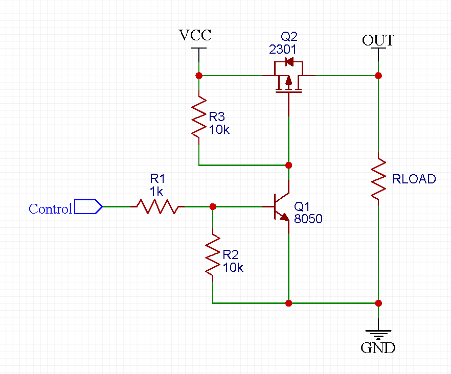
(figure 1)
As shown, the Control level controls the conduction of the Q1 transistor, which in turn controls the conduction of Q2 to achieve VCC output to OUT.
This is often the last line of defense. If the MCU crashes or runs away, resulting in control failure, it may cause serious consequences of back-end burning. Is there a way to achieve high reliability and automatic protection when the MCU crashes or runs away?
We consider that when the MCU crashes or runs away, the level is fixed. It is precisely because of this that it will lead to a situation of loss of control. So can we use a form with an unfixed level as a marker for the normal operation of the MCU? Just like some LED indicators, when flashing, it means normal.
That is to say, when the control signal of the above figure is a square wave, it represents normal, and Q2 is turned on. When Control is at a fixed level, it represents an abnormality and Q2 does not conduct. This will enable perfect protection.
How to implement this circuit?
The conduction of Q1 and Q2 is up, and a fixed level is needed for control. If you change the Control (Figure 1) directly into a square wave, the OUT output will also become a square wave.
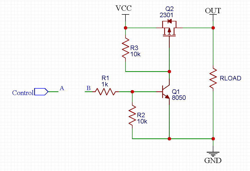
(figure 2)
Taking Figure 2 as an example, it is necessary to input the square point of the Control connection into a square wave, which becomes a high level at point B, and turns the high level and low level inputs into a low level.
First of all, we have to solve the point A when the input is high or low, point B is low. What form of circuit can solve this problem? capacitance!
So we try this circuit -
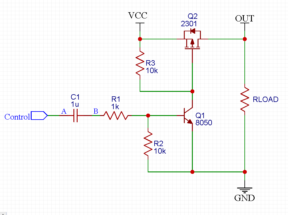
When this can really solve the high or low input, the output of point B is low.
But when the square wave is input, the problem still exists.
How to turn the square wave into a high level on the basis of the above? Capacitor integrating capacitors can be utilized. The square wave is used to charge the capacitor and convert it to a DC level. So we modified it to the following circuit -

But the actual test will find that this does not solve the problem. C2 cannot be charged. The reason is because the current will flow back from C1. So how do you solve the problem of backflow? Single-pass, that is diode .

It has been found that after adding the D2 diode, there is no way to achieve the expected voltage at point B. The actual output here is negative pressure. Therefore, a return channel must be provided.
Then modified again -
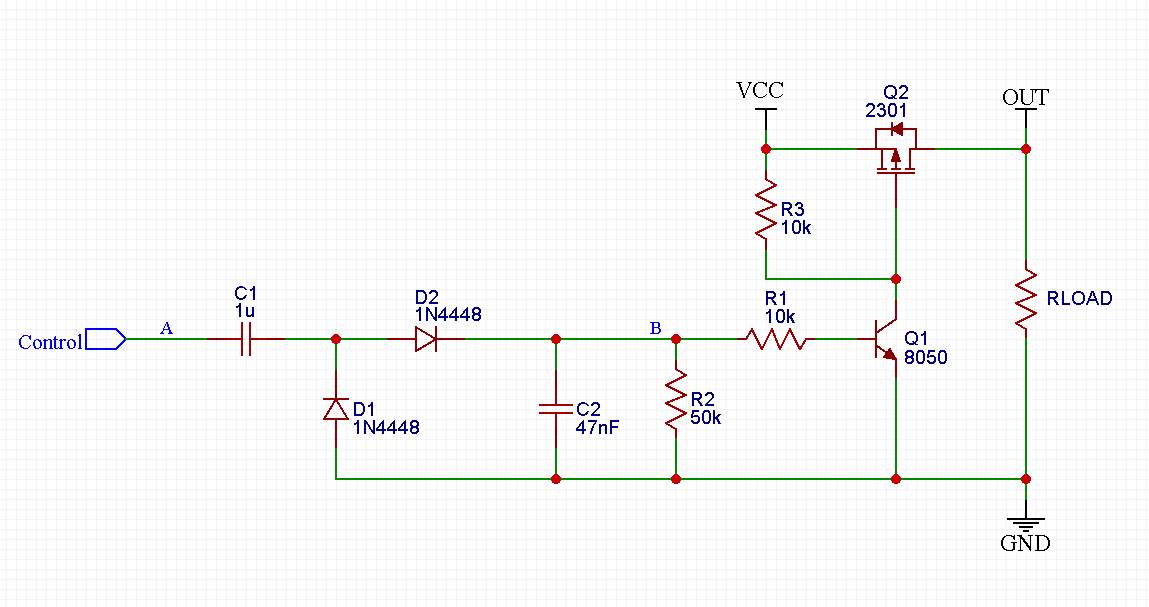
In addition to increasing D1, the order and resistance of R2 and R1 are also adjusted, and the capacitance of C2 is adjusted. The resistance adjustment is to reduce the resistance shunt, making the capacitor charge faster. R2 also plays a very important role. When the input of point A is DC level, the energy on C2 can be consumed by R2, so that Q2 is turned off.
Above, this circuit is designed. We can see through simulation -
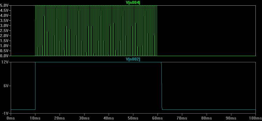
The green waveform is the A point input waveform and the blue waveform is the Out output waveform. As you can see, the above circuit is very good at fulfilling the requirements.