 0
0


 0
0


I do not know when you debug the circuit, have encountered this situation, that is, all the components on the board parameters and welding are correct, but after the power, some components in the circuit immediately damaged. This phenomenon probably has something to do with a hidden object in the circuit - parasitic inductance.
As the name suggests, parasitic inductance refers to the inductance parasitic on the PCB wiring or other components of the circuit board. Generally speaking, there will be a parasitic inductance where there is a wire, such as the copper wire on PCB, through the hole, even the bonding wire inside the chip will have a certain amount of parasitic inductance, the inductance of these parasitic inductors is generally from a few nH to dozens of nH.
● LP6451 synchronous Buck circuit is used to introduce the influence of parasitic inductance on the circuit.
Figure 1 is the typical application schematic diagram of LP6451, LP6451 uses COT control architecture, support the maximum 18V DC input, can provide the maximum 3A load current, at the same time LP6451 also integrated input undervoltage protection, output short-circuit protection, overcurrent protection, overtemperature protection and other functions, with excellent electrical performance, good safety and other advantages, Is a very cost-effective synchronous buck control chip.

Figure 1: Schematic diagram of typical application of LP6451
Effect of parasitic inductance on input.
At the input end of LP6451 scheme, two ceramic capacitors C2 and C3 will be placed to filter the input voltage and stabilize the input voltage. On the PCB board, the two ends of the circuit from the input end to the capacitors C2 and C3 are connected by the PCB wiring, which is actually the existence of parasitic inductance. We use the simulation software to see what changes will occur at the input end when the circuit is on after the introduction of 20nH parasitic inductance L1.
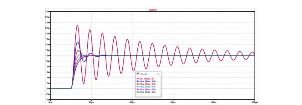
As can be seen from the simulation results in Figure 2, when the blue input voltage increases from 0V to 12V, the voltage on capacitor C1 does not rise to a stable 12V, but becomes an oscillating sine wave, and the peak voltage of the sine wave reaches 24V, which is twice the input voltage of 12V. If this voltage exceeds the maximum voltage tolerance of the components in the circuit, it will cause them to fail.

Figure 2: Simulation results
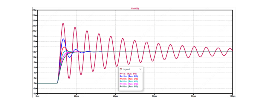
At this point, many engineers may ask, why do we not always see this oscillation in the input capacitance in practical applications? This is because in addition to the introduction of parasitic inductance, the PCB wire also introduces an additional resistance, and this resistance acts as a damping damping effect on the sinusoidal oscillation. On the basis of the previous simulation circuit, we added resistor R1. It can be seen that with the increase of resistor R1 resistance, the voltage attenuation rate on the input capacitor becomes faster and the maximum voltage also decreases rapidly.

Figure 3: New simulation results
Although the voltage oscillation caused by the parasitic inductance at the input end can be alleviated by the parasitic resistance at the same time, we should always pay attention to the voltage waveform on the input capacitor at the moment of power-on when designing the power supply, so as to avoid abnormal high voltage and damage to the circuit elements behind the input capacitor.