The new LTC2274 high-speed serial interface significantly reduces the number of parallel data lines required for a 16-bit ADC or 16-bit CMOS LVDS with 16-bit input / output (I / O) data lines on the FPGA, enabling automatic single clock, 2.1 Gbps transmission frees up valuable FPGA pins. Serial data communication provides a simplified design and requires a smaller board layout area, while providing flexibility across analog and digital boundaries. In noise-sensitive applications, the serial interface provides a barrier to effective isolation between digital and analog circuits, eliminating coupling between digital outputs and reducing digital feedback.
Serial coding according to 8B10B instruction manual JEDEC interface (JESD204) and high-speed interface of Xilinx Rocketry IO to output data converter LTC2274 serial data, supporting many FPGAs, Altera's Stratix II GX I / O and Lattice ECP2M I / O For 2.1 Gbps, the LTC2274 provides the fastest high-speed serial interface for any ADC on the market today. Leading communications teams, multi-channel systems, space-saving designs, and instrument applications will all benefit from the unique interface and feature set of the LTC2274. The LTC2274 provides several unique features to improve the overall system design. For applications with high receiving sensitivity, the LTC2274 provides a transparent internal oscillator circuit that increases the ADC's response to SFDR, which is much lower than the low-level input representing 100dBc.
To avoid interfering with the serial digital output, an optional data encoder can be used to randomize the spectrum of the serial link. A serial test mode is also integrated to test the serial interface. Although the LTC2274 can operate at sampling rates up to 105Msps, the internal PLL can be configured to block one of three different sampling frequency ranges. On-chip clock cycle stabilization circuits have been implemented to increase the duty cycle instead of 50% of the clock. It provides separate analog and digital disconnect pins to save energy. The LTC2274 Linear Technology maintains the high performance advantage, which is 77.5dB (SNR) and spurious-free dynamic range (SFDR) performance in 100dB baseband, which provides excellent signal-to-noise ratio. The ultra-low instability of 80fs RMS results in undersampling of input frequencies up to 500MHz and excellent noise performance. The LTC2274 consumes 1.3W of a 3.3V analog power supply.
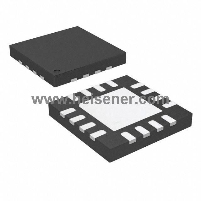
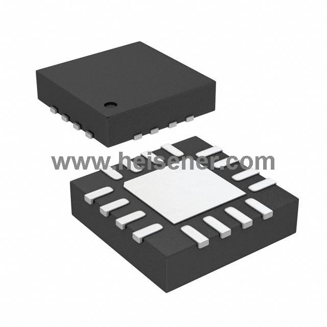
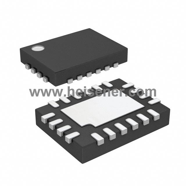
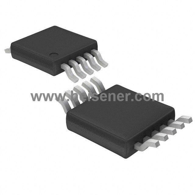
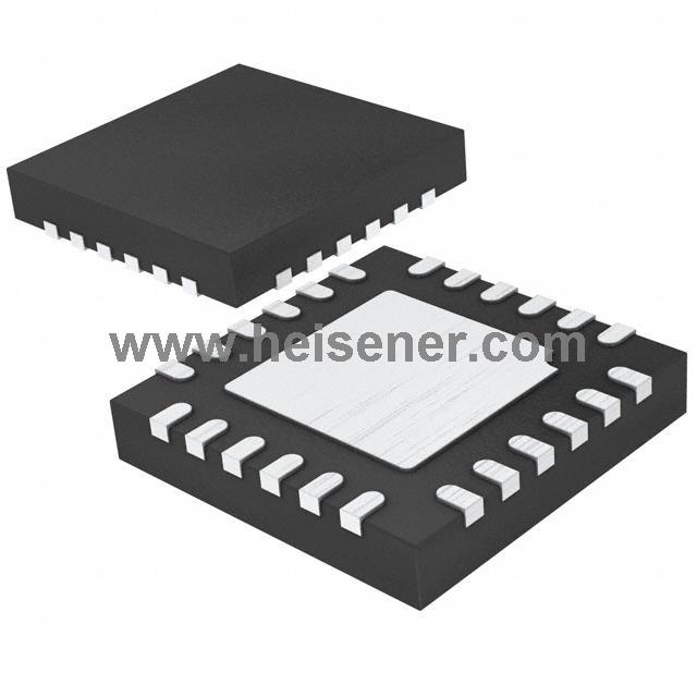
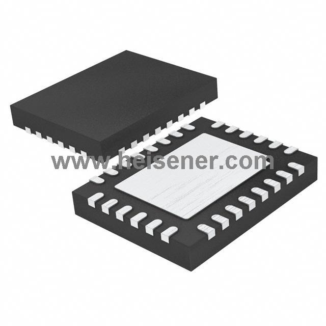
The LTC2274 series output can be mounted in a 6mm x 6mm QFN-40 package, similar to the average of less than 16-bit ADCs with parallel outputs. In addition to the 16-bit 105Mps LTC2274, a pin-compatible 80Msps version and 65Msps will be released this summer. Production of the LTC2274 will be available at commercial and industrial temperatures in July.
 0
0


 Login/Register
 BOM
BOM
 Cart
Cart


