2N5551 Introduction
The 2N5551 is an NPN bipolar junction transistor designed primarily for high-voltage, low-current applications. It is widely used in electronic circuits for its ability to handle relatively high voltages and moderate current levels. The transistor features a high collector-emitter voltage rating of up to 160V and a maximum collector current of 600mA, making it suitable for various switching and amplification purposes.
The working principle of the 2N5551 revolves around current amplification. When a small current flows into the base terminal, it allows a much larger current to flow from the collector to the emitter. This occurs because the base-emitter junction is forward biased, allowing electrons to move from the emitter to the base. Meanwhile, the base-collector junction is reverse biased, which enables most of these electrons to be swept into the collector. This mechanism allows the transistor to act as a current amplifier, where a small base current controls a larger collector current.
2N5551 Pinout

Pin1 (Emitter): This terminal is usually connected to the GND terminal, allowing the current to flow out through this terminal.
Pin2 (Base): This pin is responsible for controlling the transistor's biasing, thereby regulating the transistor's operation.
Pin3 (Collector): This terminal is connected to the load and provides the pathway for current supply.
2N5551 CAD Models
Symbol

Footprint

3D Model

2N5551 Circuit Diagram

2N5551 Marking Diagram

2N5551 Specification
| Parameter |
Value |
| Transistor Type |
NPN |
| Collector-Emitter Voltage |
160V |
| Collector-Base Voltage |
180V |
| Emitter-Base Voltage |
6V |
| Collector Current |
600mA |
| Power Dissipation |
625mW |
| DC Current Gain |
80-250 |
| Transition Frequency |
100MHz |
| Operating Junction Temperature |
-55°C -150°C |
| Package |
TO-92 |
| Saturation Voltage |
0.3V (max) @ 10mA |
| Base Current |
200mA (max) |
2N5551 Features
Pb−Free Packages are Available
General Purpose Switching Application
Withstand a collector-emitter voltage (Vceo) of up to 160V
Supports a maximum collector current (Ic) of 600mA
The transistor has a DC current gain (hFE) range of 80 to 400
The transition frequency (ft) is 100 MHz
It has a power dissipation (Pd) of 625mW
2N5551 Applications
Audio Amplifiers
Signal Amplifiers
Switching Regulators
Relay Drivers
LED Drivers
Voltage Regulators
Oscillators
Timers
General Switching
Biasing Circuits
Modulation Circuits
RF Transceivers
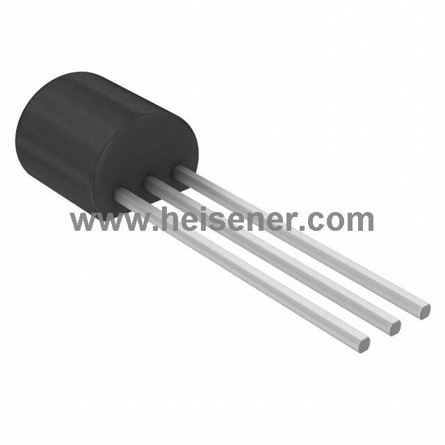
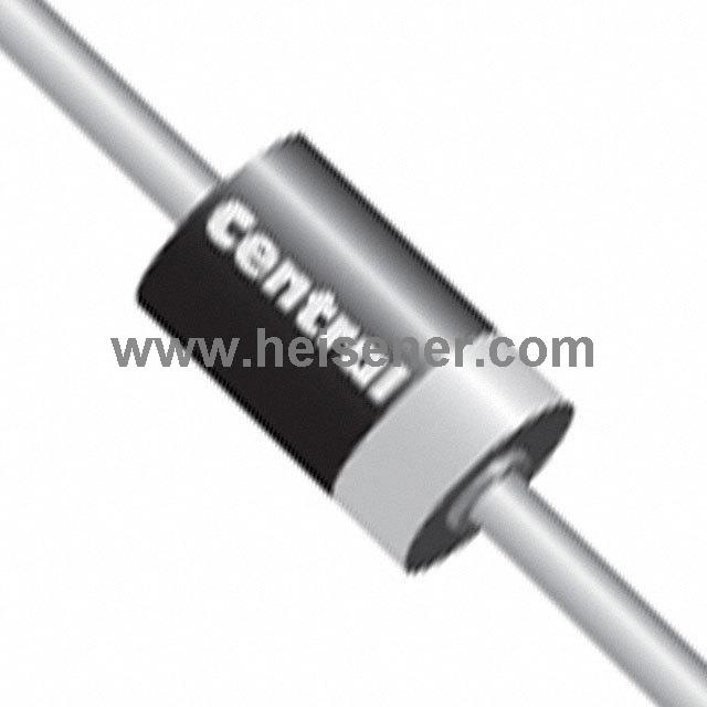
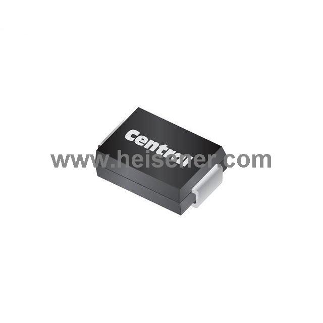
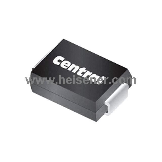
2N5551 Package

How to Use 2N5551?
When the 2N5551 is properly biased, the emitter current is the sum of the currents through the base and collector terminals. For proper operation, the voltage at the base terminal must be positive relative to the emitter to allow current to flow from the emitter to the collector. The performance of a transistor is characterized by its forward current gain, Beta (β), which is the ratio of the collector current (I_C) to the base current (I_B). For 2N5551, β is typically between 20 and 1000, with a typical value of about 200. Another key factor is the current gain, alpha (α), which is the ratio of the collector current (I_C) to the emitter current (I_E), and is typically between 0.95 and 0.99.
To use the 2N5551 in a circuit, first determine the necessary biasing to ensure that the base-emitter voltage (V_BE) is approximately 0.7V. Calculate the required base current (I_B) for the required collector current (I_C) using I_B = I_C / β. Ground the emitter, connect the collector through a load to the positive supply voltage, and apply the calculated base current to the base through a resistor to limit the current. The base resistor (R_B) can be calculated using Ohm's law: R_B = (V_CC - V_BE) / I_B, where V_CC is the supply voltage.
FAQs
Can the 2N5551 be used in a Darlington pair configuration?
Yes, the 2N5551 can be used in a Darlington pair configuration to achieve higher current gain, combining the β of both transistors for significantly increased amplification.
Are there any equivalents to the 2N5551 transistor?
Yes, equivalent transistors to the 2N5551 include the 2N555L, 2N5551D26Z, 2N5551TRE, 2N5551RL1G, 2N5551RLRA, 2N5551-AMMO, 2N5551RLRM, 2N5551RLRP, 2N5551-AP and 2N5551STOB, which can be used as substitutes in similar applications.
How should I handle the 2N5551 to avoid damage from static electricity?
Handle the 2N5551 using proper anti-static precautions, such as grounding yourself, using anti-static wristbands, and working on anti-static mats to prevent damage from static discharge.
 0
0


 Login/Register
 BOM
BOM
 Cart
Cart