Post Date: 2015-06-01

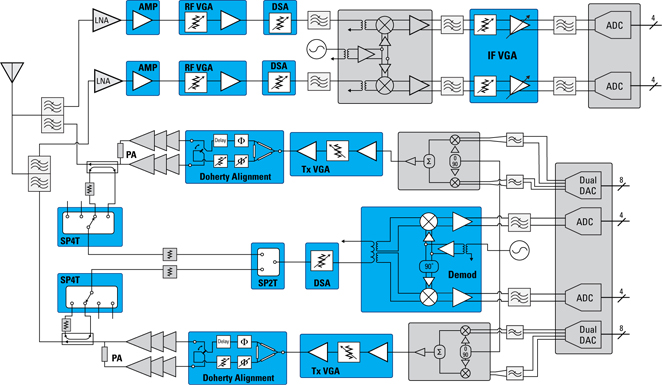
The rapid development of equipment technology may cause people to question established design best practices. Until recently, engineers designing RF and microwave circuits for applications such as 4G base stations, broadband repeaters, or distributed antenna systems will still automatically select GaAs FETs to achieve the best noise figure and linearity. Silicon-based devices will rarely be considered. But now, as issues of size, cost, reliability, and settling time become more important, and as technology advances enhance key aspects such as noise, distortion, and transient response, silicon can provide an excellent Solution (Figure 1).
GaAs strengths and weaknesses
GaAs technology has been a key driver of the wireless revolution. It has a low noise figure and high linearity, surpassing the capabilities of today's silicon devices. Since noise figure and linearity are the main factors that determine the overall distortion introduced in the system by key functions such as variable gain amplifiers, digital step attenuators, switches, mixers, and modulators, it is usually the default Selecting a GaAs device with the best signal performance is required.
As a more specialized technology than conventional silicon-based manufacturing, GaAs is relatively limited in its application to pure analog functions. Including digital circuits often requires designing multi-die modules on laminated substrates. This is expensive and results in reduced humidity sensitivity and therefore requires special storage and handling. GaAs-based modules typically have an MSL3 sensitivity rating, so they must be used within one week after sealing to ensure that moisture absorption does not damage the device, leading to early failure. However, silicon-based ICs are usually implemented as QFN monolithic chips, so they have a lower MSL1 sensitivity level, can be shipped on standard reels, and require no special processing.
In addition, GaAs devices have relatively low ESD-they typically only withstand 500V Human Body Model (HBM) thresholds. In comparison, the comparable silicon component is 2kV. As a result, GaAs devices are easily damaged by low-level ESD events that occur in typical assembly areas. Much less antistatic measures are required for similar silicon devices. Silicon-on-insulator (SOI) switches also typically have an excellent RON x COFF figure of merit, so they have lower insertion loss and greater isolation.
Finally, circuits containing GaAs devices often rely more on external passive components, such as inductors and resistor components, which take up more space and increase the complexity of the solution.
Figure 1. Base station radio block diagram showing how and where silicon can replace GaAs (indicated in blue) to provide better reliability, integration, and cost in high-performance RF equipment, gates in GaAs switches Delays are
used in infrastructure equipment for high data rate 3G and 4G communication systems and other industrial systems, requiring RF transistors to stabilize quickly after switching to meet critical time performance or maintain signal integrity. Settling time is affected by the gate delay associated with the switch. The gate hysteresis experienced when the switch is turned on can be regarded as the difference between the point where the switch resistance is completed in 10-90% rise time and the point where the switch can be considered to be completely stable. Usually, this is opened between 97.5% and 100%. The gate lag can also be seen as the time difference between the 90% amplitude of the RF power output from the device and the fully stable to 100% amplitude.
It is well known that GaAs devices have considerable gate hysteresis, which can limit system performance, especially when operating at lower ambient temperatures. High-speed communication systems must wait for this settling time before they can begin transmission. Longer settling times may limit the speed and agility of the system, and also increase the duration of tests in a production environment.
Silicon closes performance gaps
Despite the known shortcomings of gallium arsenide (GaAs), superior noise figure and third-order intercept (IP3) linearity typically overcome these shortcomings compared to silicon. But now, with new technologies that help overcome traditional limitations, silicon devices can provide a more robust alternative, providing the opportunity for a more economical and reliable solution. New generation RF switches using SOI technology (such as IDT's F2912) can reliably operate in high temperature environments on or near PA components. These new silicon switches provide excellent performance at temperatures up to + 120 �� C (0.4 dB insertion loss, +65 dBm IP3, 60 dB isolation) (Figure 2a).
Figure 2a. High Rel SOI switching performance (F2912).
New generation silicon IF variable gain amplifiers (VGAs) such as IDTF1240 have made breakthrough improvements in SNR by using FlatNoise technology. FlatNoise can ensure that even if the gain is reduced, the noise figure remains low (Figure 2b). In the past, engineers had to accept the past that the noise figure was reduced by 1 dB for every 1 dB of gain reduction. As a result, the system SNR can be increased by up to 2 dB, while still maintaining high linearity.
Figure 2b. Impact of FlatNoise technology on IF VGA noise figure (F1240).
Linearity is another important parameter that has recently improved significantly in silicon devices. IDT's F0480 silicon-based RF VGA has a new zero-distortion technology, which can achieve a bandwidth of 2000dBm at 40dBm OIP3 and an adjustment range of 23dB when the quiescent current is only 100mA (Figure 2c). Generally, improving the linearity and bandwidth of a VGA provides designers with greater flexibility to implement a receiving system.
Figure 2c. New wideband silicon RF VGA (F0480) with zero distortion technology.
By developing glitch-free technology, IDT also overcomes important flaws that affect digital step attenuators (DSAs). Glitch-free reduces the known transient overshoot that occurs when the MSB state transitions from 10dB to only 0.5dB (Figure 2d). In precise level setting environments such as transmitters, this technique ensures a smooth transition of gain to adjacent settings. Historically, larger 10dB glitches have been able to damage downstream power amplifiers. In addition, traditional DSAs take a long time to resolve, which reduces the turnaround performance of time domain duplex (TDD) systems. By almost eliminating this overshoot, Free-Free can significantly improve system reliability and support more flexible TDD systems.
Figure 2d. Burr-free SOI DSA (F1950).
Conclusion
GaAs amplifiers and switches have high linearity and good noise characteristics, making this technology the default choice for designers of high-performance RF equipment. Although silicon-based devices have advantages in terms of reliability, integration, and cost, the superior performance of these areas in the past has ensured GaAs status. Recently, these factors have become increasingly important, which has led to new interest in the use of silicon-based devices. With the help of new technologies such as SOI, zero distortion, and glitch-free, with the improvement of noise performance and linearity, this technology has now become an attractive alternative to GaAs.
 0
0


 Login/Register
 BOM
BOM
 Cart
Cart

