 0
0


 0
0


The DS1020 programmable 8-bit silicon delay line consists of an 8-bit user programmable CMOS silicon integrated circuit. The delay value, programmed using a 3-wire serial port or an 8-bit parallel port, can vary in 256 equal steps. The fastest model (-15) has a maximum delay of 48.25 ns with an incremental delay of 0.15ns, while the slowest model (-200) has a maximum delay of 520ns with an incremental delay of 2ns.
Functional block diagram

All models have an inherent (step size zero) delay of 10ns. After a user-determined delay, the input logic state reappears at the output without inversion. Compatible with TTL and cmos, the DS1020 is capable of driving 10 74ls type loads with rising edge and falling edge accuracy.
The full cmos DS1020 integrated circuit is designed as a reliable, economical alternative to hybrid programmable delay lines. It offers a standard 16-pin automatic insert DIP and a space-saving surface mount 16-pin SOIC.
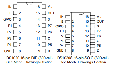
Pin assignment

Pattern description
Parallel mode (s =1)
In parallel programming mode, the output of the DS1020 will reproduce the logical state of the input after a delay determined by the state of the eight program input pins P0-P7. Parallel inputs can be programmed using DC levels or computer-generated data. For infrequent changes to the delay value, you can use jumpers to connect the input pins to VCC and ground.
For applications that require frequent timing adjustments, use dip switches. In a hardwired implementation, the enabling pin (E) must be located in logical 1. Maximum flexibility is achieved when the eight parallel programming bits are set using computer-generated data. Enable pins can be used to latch data provided on the 8-bit bus when data setting (tDSE) and data retention (tDHE) requirements are observed. If not used to latch data, Enable must remain on logical 1. After each delay value change, a stabilization time (tEDV or tPDV) is required before the exact delay input logic level.
Since the DS1020 is a CMOS design, unused input pins (D and C) must be connected to well-defined logic levels; They must not be allowed to float.
Serial mode (s = 0)
In serial programming mode,DS1020 will copy the logic state output into serial port d after the delay time monitored by an 8-bit value, observe the data setting (tDSC) and data (tDHC) requirements, timing the data loading in the MSB-to-LSB order of the front serial clock (C), so that the pin (E) must be loaded in logic 1 or the internal input 8 Bit registers are read, during which the delay is activated by the last value.
When enable (E) returns logical 0, the data transfer ends and a new delay value is activated. After each change, a stabilization time (tEDV) is required before the delay is accurate. When the order value is moved to the serial data input (D), the previous contents of the 8-bit input register are moved out of the serial output pin (Q) in the order msb to lsb. Multiple devices can be programmed via a Daisy chain (cascade) by connecting the serial output of one DS1020 to the serial input of another DS1020 (See the picture below).
Multi-device cascade (Daisy chain)

The total number of serial bits must be 8 times the number of Daisy chain units, and each set of 8 bits must be sent in msb to lsb order. The application can read the Settings for the DS1020 delay line by connecting the serial output pin (Q) to the serial input (D) with a resistor with a value of 1k to 10k ohm (See the picture below).
Continuous readout

Because the reading process is destructive, the resistor recovers the value read and provides isolation when writing to the device. The resistor must connect the serial output (Q) of the last device to the serial input (D) of the first device in the Daisy chain. For serial readouts that are automatically recovered by resistance, the device used to write serial data must enter a high impedance state. To start a serial read, enable (E) is brought to logical 1 and the serial clock (C) is located at logical 0. After the wait time (tEQV), bit 7 (MSB) appears on the serial output (Q). On the first rise (0→1) transition of the serial clock (C), bit 7 (MSB) is overwritten and bit 6 appears on the output after the time tCQV.
This clock process must be repeated eight times in order to restore the input register to its original state. In the case of Daisy chains, this process must be repeated eight times per pack. If the read value is restored before enable (E) returns logical 0, no time (tEDV) needs to be set, and the programming delay remains the same. Since the DS1020 is a CMOS design, unused input pins (P1-P7) must be connected to well-defined logic levels; They must not be allowed to float. The serial output Q/P0 should be allowed to float if not used.
Features
● All-silicon time delay
● Models are 0.15ns, 0.25ns, 0.5ns, 1 ns, 2ns step size
● Programmable using 3-wire serial port or 8-bit parallel port
● Leading edge and trailing edge accuracy
● Standard 16-pin DIP or 16-pin SOIC
● Economy
● Automatic insertion, low profile
● Low power CMOS
● TTL / CMOS-compatible
● Gas phase, infrared and wave welding
Test setup instructions
The following figure illustrates the hardware configuration used to measure the timing parameters of the DS1020. The input waveform is generated by a precision pulse generator controlled by software. The time delay is measured by a time interval counter (20 ps resolution) connected to the output. The DS1020 serial and parallel ports are controlled by an interface connected to a central computer. All measurements are fully automated and each instrument is controlled by computer via IEEE 488 bus.
Dallas semiconductor test circuit
