Post Date: 2015-06-01

The shift from a vertically integrated to an architecture based on an extended third-party supply chain has increased cost-effectiveness, but has created risks for electronic original equipment manufacturers. The particular risk posed by this shift is the task of securing intellectual property. In design.
Individuals, criminal networks, and even governments are involved in attempts to unlock electronic systems for financial gain or future tactical advantages to unlock the secrets of electronic systems. Pirates may provide almost identical counterfeits and considerable profits; competitors may use your IP to start their own efforts; opponents may use information obtained from the system to weaken it when they see an opportunity.
Field programmable gate arrays (FPGAs) have become the main targets of these attacks. FPGAs are now widely used in systems that previously required hard-wired ASICs or microcontrollers. Improvements in process technology have increased the number of gates to millions; this way, a complete system with an FPGA at its core can be built. The increase in logic density allows FPGAs to provide processors and custom logic for most of the system. This transition to programmable solutions has changed the way engineers need to consider design security while protecting the organization's IP and reputation.
There are many ways to compromise design security. One is reverse engineering. Once the logic function of the chip is determined, pirates can copy the system or mix other functions to realize a new system that is sold at a higher price than the original product. Both ASICs and FPGAs are susceptible to this approach, but it is possible to use the capabilities of FPGAs to make reverse engineering more difficult for competitors.
The layout of the ASIC can be obtained by removing the cover of the device and gradually peeling off the metal interconnection layer of the device. Although this is a time-consuming process, reverse engineering teams can use the tools available to extract viable netlists from layout information obtained through destructive analysis. For FPGAs, instead of performing reverse engineering using destructive analysis, it is done by extracting a configuration bitstream.
The most common FPGA technology used today is SRAM-based, which is fast and reconfigurable, but must be reconfigured every time the FPGA is powered on. Generally, an external programmable read-only memory (PROM) is used to save the configuration data of the FPGA. Configuration data can be intercepted and read during boot. Although the configuration data is not human-readable, automatic analysis can be used to reconstruct the netlist to support reverse engineering of the IP.
The ability to read the configuration bitstream enables two other forms of commercial piracy: cloning and overbuilding. If pirates are only trying to imitate the design to produce counterfeit products, cloning is the method they are most likely to use. FPGAs in a given product are most likely to be available on the open market. In this way, pirates can simply obtain the configuration bitstream and program the PROM of the FPGA to produce functional counterfeit products.
Overbuilding is closely related to cloning and is one of the easiest forms of piracy. When the number of systems manufactured by the contract manufacturer exceeds the required number of systems, overbuilding occurs. Because the components of the entire system are likely to be available from multiple sources, it is often easy for manufacturers to order a complete bill of materials that duplicates the original design. The contract manufacturer will most likely not need to extract the configuration data from the on-board ROM, as OEM customers are likely to have sent them the necessary information.
Issues related to design security are features designed to prevent service theft. Many electronic devices are designed to provide secure services using secure transactions. In many cases, the revenue from the service provided the majority of the supplier's profits. The hardware itself can be sold for less than the cost. To maintain a source of revenue, vendors need to ensure that users can only get services after payment. If users bypass the payment mechanism, it will result in severe loss of revenue and profits.
If hackers are able to obtain detailed information about the implementation of encryption, they are more likely to crack the encryption keys processed by the system, thereby breaking the protection mechanism. The technique of cracking encryption is not limited to conventional reverse engineering (Figure 1). Analyzing side-channel information (power consumption or EMI by the heat sink) can provide important clues about the processing steps performed by the cryptographic processing unit. The technology is so pervasive that it prevents competition among security researchers. To date, the competition has been held three times to find the fastest researchers to find protected keys on standard systems.
Figure 1. Side-channel information analysis can provide important clues that can help hackers crack FPGA cryptography.
FPGA manufacturers have introduced many device-specific security measures to prevent various forms of counterfeiting and help prevent unauthorized unlocking of IP and services.
FPGA's first line of defense is mainly in bitstream encryption. In addition to the ambiguous configuration of the bitstream format itself, this provides an additional layer of protection. Altera, Lattice, and Xilinx FPGAs currently provide on-chip decryption hardware for configuration data. Usually, the bitstream is encrypted by the manufacturer using the AES algorithm. The AES algorithm is based on the Rijndael algorithm. It is a symmetric 128-bit data block cipher, using 128, 192, and 256-bit cipher keys. Symmetric means that the same key is used for encryption and decryption. Each 128-bit input block (a 4-by-4 2-D byte array, also known as a state) goes through a sequence of four byte-oriented block transformations, and how many rounds each transformation passes depends on the used Key length. AES-128 is 10 rounds,
and the conversion used is:
byte replacement row byte shift, by adding 0 to 3 to increase the mixing of the columns in the state array. Add the corresponding round key to the state.
During board assembly and programming, a 256-bit key is written to the target FPGA. During the boot process, the AES block gets the bitstream, decrypts it, and then passes the configuration data to the configuration logic. Since plain text configuration data is not visible on any I / O port, pirates cannot read the stream. Instead, they must use powerful computers to spend a lot of resources on bitstream decryption.
FPGAs differ in how they store keys. Low-cost SRAM-based FPGAs typically store data in SRAM, which requires battery backup to protect the keys when the system is powered down. More advanced SRAM-based FPGAs use one-time programmable (OTP) memory to hold keys, eliminating the need for a battery backup. Another method of encryption is to store the configuration on the FPGA itself. Therefore, the only time the bitstream can be read is in the factory where it is programmed. Some devices, such as Lattice ECP2 FPGAs, contain an on-chip flash memory that can be assigned to configuration data. At startup, only the internal bus is used to copy the configuration data into the SRAM cell that controls the internal state of the FPGA.
Figure 2. Some FPGAs, such as the Lattice MachXO2 shown here, store configuration data on the FPGA itself.
Microsemi's devices are a step forward in non-volatile configuration technology. With anti-fuse and flash-based gates, no large-capacity configuration bitstreams need to be protected. This not only provides advantages at power-on, but also ensures that there is no way to read out the bit stream after programming.
Flash-based devices in the Microsemi portfolio increase security by providing many key storage and management options. These options help prevent tampering that could compromise data, service security, or any attempt to analyze the internal state of the FPGA.
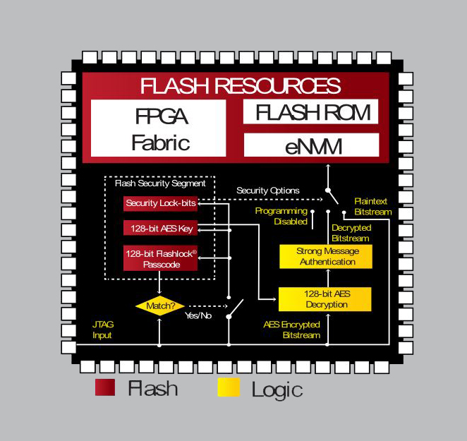
With flash-based devices, user encryption keys can be stored permanently without the need for a backup battery. Many Microsemi Flash-based device architectures use non-volatile memory security blocks. This memory can only be written from the device programming interface, not from the FPGA. For the SmartFusion series, it cannot be written from the on-chip microprocessor. This helps make the device more resistant to attacks (a common technique) initiated through the system bus.
Figure 3. Many Microsemi Flash-based device architectures use non-volatile memory security blocks. This memory can only be written from the device programming interface.
The security lock bit setting may, for example, require subsequent upgrades to be encrypted with the correct key. Alternatively, this can prohibit the upgrade without first having to unlock it with a valid password. You can also permanently disable the upgrade, so that the device can perform OTP effectively.
The segmented nature of key and password storage in Microsemi's family of flash-based devices enables different participants in the supply chain to participate in device programming at different times. If only part of the supply chain can be trusted, this will provide a way to effectively manage security (Figure 4).
Figure 4. Example of an FPGA security configuration process.
For example, Microsemi may have a flash segment configured at the factory. This can be used to store keys that allow loading of licensed third-party IP cores. The design owner can configure another segment, such as the bitstream decryption key and security options; the contract manufacturer can then apply the configuration to the main FPGA fabric. Finally, end users can configure Flash ROM segments, for example, to load application-level encryption keys that control user service access.
To prevent a running system from being attacked, FPGA manufacturers have implemented countermeasures. For example, Altera has tamper protection on many of its FPGAs. If a control fuse is set, the device will only accept a configuration bitstream encrypted with the correct key. This prevents an attacker from trying to determine the functionality of other parts of the system by changing the FPGA configuration. Stratix, Cyclone, and Arria devices can also be set to regularly monitor internal configurations to see if they match the checksum. This prevents an attacker from overwriting the logic to see how changes affect system behavior. Stratix devices can also be configured so that if the system logic has tamper-detection capabilities, it can issue commands to clear the entire FPGA memory.
In order to prevent side-channel attacks, Microsemi has designed multiple designs Technical licenses were obtained from the Security Experts Office. Its latest AES implementation on flash-based devices has been highly resistant to such attacks. Customers can use licensed countermeasures in their own safety logic functions.
Although FPGAs appear to be more vulnerable to cloning, counterfeiting, and tamper-based attacks, silicon vendors have enabled customers to implement effective countermeasures. Now, the different types of FPGAs available allow one to choose the level of design security required by almost any application.
 0
0


 Login/Register
 BOM
BOM
 Cart
Cart

