 0
0


 0
0


TDA4605 Introduction
The TDA4605 is a highly efficient integrated circuit designed for controlling MOS power transistors in free-running flyback converters, making it an essential component for modern power supply designs. It combines advanced regulation and monitoring functionalities to ensure stable and reliable operation across a wide load range. This versatility makes it ideal for both consumer electronics and industrial applications, where precise load regulation is critical.
The IC's ability to manage power efficiently while maintaining system safety and reliability ensures optimal performance, particularly in demanding environments that require robust and adaptable power supply solutions.
TDA4605 Pin Connection

Regulating Voltage (Pin 1): Input for secondary voltage regulation. It compares the voltage from the transformer’s regulating winding to an internal reference, adjusting the pulse width at Pin 5 based on load conditions such as normal operation, overload, short circuit, or no load.
Primary Current Simulation (Pin 2): Input for simulating primary current rise as a voltage ramp using an external RC network. This pin terminates the pulse at Pin 5 when the simulated voltage reaches a value derived from Pin 1, setting the maximum power for overload conditions.
Primary Voltage Detector (Pin 3): Input for primary voltage monitoring. The IC shuts down when voltage at Pin 3 is below an internal reference. It also compensates for the overload point.
Ground (Pin 4): Common ground reference for the IC.
Output (Pin 5): Push-pull output for driving the gate capacitance of the power MOS transistor.
Supply Voltage (Pin 6): Input for IC power supply. Derives an internal reference voltage and supply voltage detection thresholds. It enables VREF and logic operation within defined voltage ranges.
Soft-Start (Pin 7): Input for start-up and regulation integration. A capacitor connected here enables soft-start with short pulses and functions as part of an integrator network.
Zero Detector (Pin 8): Input for oscillator feedback. Each zero-crossing of the feedback voltage triggers an output pulse at Pin 5, ensuring precise timing with a typical threshold of -50mV.
TDA4605 Symbol

TDA4605 Footprint

TDA4605 3D Model

TDA4605 Block Diagram

TDA4605 Specification
| Parameter | Value |
| Control Method | PWM Control |
| Input Voltage Range | 8.5V ~ 16V |
| Maximum Output Current | Depends on external MOSFET |
| Oscillator Frequency | 20 kHz ~ 100 kHz |
| Standby Current Consumption | < 2 mA |
| Operating Temperature Range | -20°C ~ 85°C |
| Package Type | 8-DIP |
| Zero-Crossing Detection | Typical threshold -50 mV |
TDA4605 Features
Provides Overload Protection for External Diodes
Burst Operation under Short-Circuit and No Load Conditions
Loop Error Protection
Switch-off in Case of Too low Line Voltage (Under Voltage Switch-off)
Line Voltage Compensation of Overload Point
Soft-Start for Smooth Start-up
Chip Over-Temperature Protection (Thermal Shutdown)
On-Chip Parasitic Transformer Oscillation Suppression Circuitry
Decrease of Regulated Voltage for Low Power Consumption
TDA4605 Applications
Power supplies
Adapters and chargers
Flyback Converters
Energy-Saving Devices
Switch-Mode Power Supplies (SMPS)
TDA4605 Package
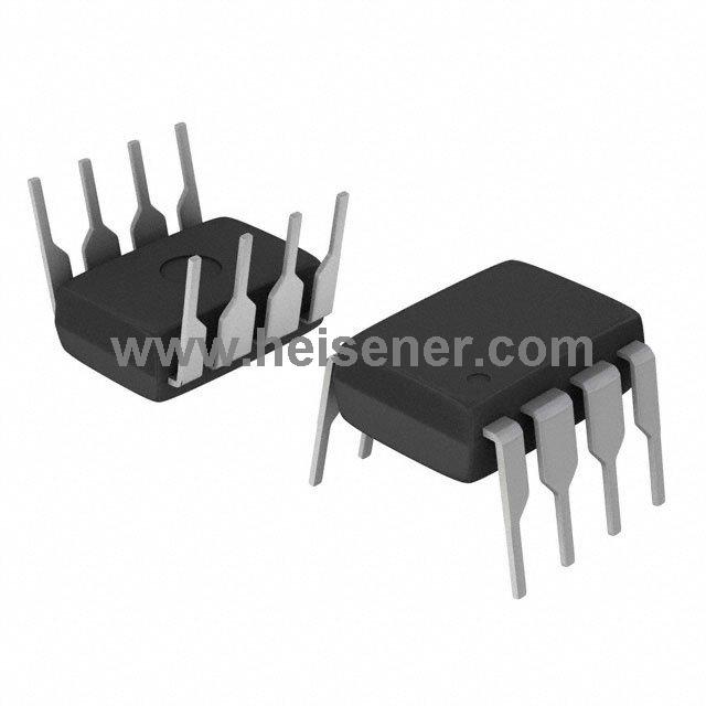
The TDA4605 is housed in an 8-pin Dual Inline Package (8-DIP), designed for through-hole mounting with compact dimensions and excellent mechanical stability. The package features a body width of 7.62 mm , a pin pitch of 2.54 mm, and a height of up to 4.57 mm, ensuring efficient PCB utilization. Constructed from high-temperature plastic with reliable thermal resistance, it supports robust performance in demanding environments.

How to Use TDA4605?
First, properly install the TDA4605 into the 8-DIP socket on the circuit board. Connect the regulating winding of the transformer to Pin 1 to provide feedback for the secondary voltage. Use an external RC network to connect Pin 2 to the primary current simulation circuit. Attach the input voltage detection circuit to Pin 3.
Additionally, connect a soft-start capacitor and resistor network to Pin 7, which will generate short pulses during startup and act as an integrator network for regulation. Link the gate of the MOSFET to Pin 5 to drive the power switch using the push-pull output function.
For power supply, connect a regulated voltage source to Pin 6 to power the IC, ensuring the voltage remains within the specified range. Upon startup, the TDA4605 triggers output pulses via the zero detector input at Pin 8 and adjusts the pulse width based on load conditions.
FAQs
What is the primary function of the TDA4605?
The TDA4605 is a control IC designed for free-running flyback converters. It regulates and monitors the MOSFET power switch, ensuring efficient power delivery and stable operation in power supply circuits.
What is the typical application circuit for the TDA4605?
It is commonly used in power adapters, industrial control systems, consumer electronics power supplies, and other applications requiring a flyback converter.
How does the zero detector work in the TDA4605?
The zero detector, connected to Pin 8, synchronizes the output pulses with the transformer feedback signal. It detects zero crossings of the feedback voltage to optimize pulse timing and energy transfer.